Electronics components such as PCBs, connectors and semiconductors rely on coatings to protect the copper surface and provide a good electrical contact. Covered by the world-class IPC guideline specifications, PCB plating thickness coating configurations rely on precise coating thickness and can include several layers to ensure the finished components perform as they should over the expected lifetime of the part.
Electromagnetic thickness gauges can give fast and reliable results for measuring copper thickness on PCBs, whereas benchtop XRF is the technique of choice when measuring gold, nickel, tin, silver, and palladium layers that form the crucial electrical contact and protect the underlying copper. The challenges posed by today’s electronics components in terms of size and complexity means that it’s important that the plating thickness equipment chosen for this application is designed specifically for electronics.

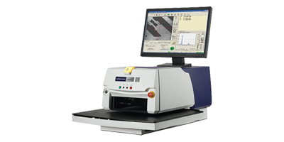
The FT200 Series XRF coatings analyzers are designed to simplify and accelerate testing of components and assemblies making it easier to measure more parts in less time. With features such as Find My Part™ smart recognition, automated sample focusing and a wide view camera, the FT230 and FT210 reduce set up time and user error to increase throughput and productivity. Let your XRF make decisions for you.

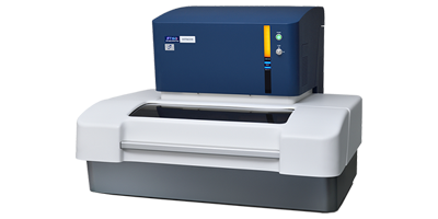
The FT160 is the one to choose for measuring nm-range layers on minute features. Advanced polycapillary optics and a state-of-the-art silicon drift detector allows you to accurately and rapidly measure nanometer-scale coatings on features smaller than 50 µm. A high-definition camera and large sample table makes it easy to locate and analyze minute features on large PCBs and semiconductor wafers, and automated feature location function cuts measurement time.

The versatility of the X-Strata920 makes it an ideal choice if you are measuring a wide range of sample types, shapes and sizes, such as PCBs, connectors and lead frames. You can choose from six collimator sizes when you make each measurement, ensuring that you get the right balance of analysis speed and thickness accuracy. You can also choose between SDD and proportional counter models depending on your application.

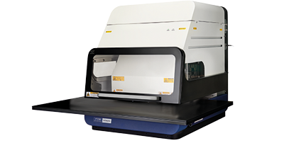
The FT110A contains powerful X-ray source and an extra-large sample chamber to accommodate large samples, such as PCBs. Automated positioning makes it easy to locate the area of interest – especially useful when analyzing minute features on large substrates. This instrument can analyze up to four layers at once, plus the substrate, making it easy to maintain coating quality when producing high volumes of electronic devices.

Choose from handheld and benchtop models of thickness gauge for PCB copper thickness measurements. With micro-resistance and eddy current models available, applications with these digital instruments include copper foil and laminate thickness, surface copper thickness and through-hole copper thickness measurements.
Watch how Hitachi analyzers can make the difference in electronics coating quality control.
Find out more about our XRF analyzers and electromagnetic thickness gauges and how they can help you meet stringent electronics quality targets.
For more information on the best instrument for your electronics coating application, get in touch to speak with one of our experts.
Contact Us