‘Which analyzer is best for my application?’
This is a question we are asked a lot. And the answer very much depends on the kind of analysis you are doing, the level of accuracy you need and what type of components you are analyzing. When your application is measuring coatings thickness on PCBs, semiconductors and connectors in electronics our answer is always ‘you need to look at the FT160’.
When it comes to analysis, electronics components are a challenge. The most obvious hurdle is that the features are so small. This itself means that you need an ultra-high precision instrument with a small spot size. And although the features may be small, the PCB or wafer may be quite large. This can mean that simply finding the feature you want to measure can be time-consuming.
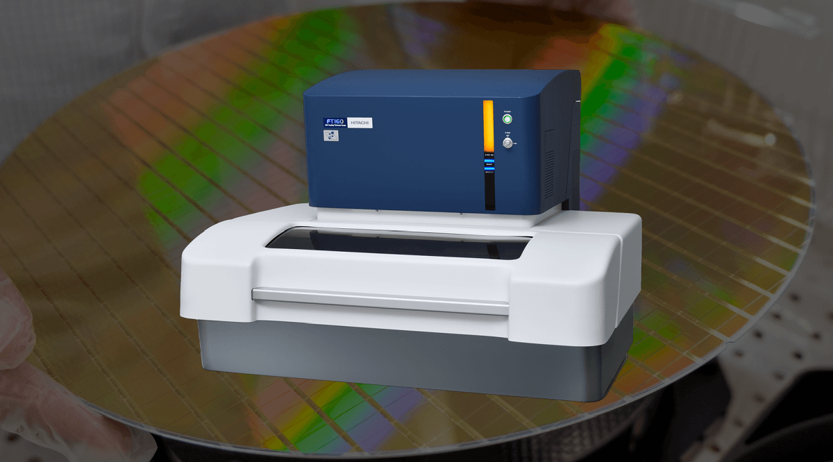
The FT160 has been developed with these challenges in mind. Designed specifically for the measurement of coatings on tiny features on large components, the FT160 includes a host of features that make coatings quality control much easier in production. Here are some of those features and why they help:
Advanced optics to precisely measure features less than 50 µm
The FT160 has an innovative polycapillary optic system that generates a high-intensity 30 µm beam for accurate measurement of the tiniest of features in semiconductor wafer and ultra-small components. And the polycapillary optics have been designed to drastically reduce the unwanted ‘halo effect’ that can cause an undesirable increase in spot size for some high-energy measurements.
High sensitivity SDD detector for accuracy at speed
The detector in your XRF instrument not only determines what you can measure, but also how quickly you can get a result. The more sensitive the detector, the better the precision and the shorter the measurement time. The FT160 includes a high sensitivity SDD detector that easily resolves the many elements present in the different layers of your component and effectively doubles the count-rate of older technology – meaning you get an accurate result fast.
Optimized sample lighting for pin-point accuracy
As we’ve mentioned previously, sometimes simply finding the right area for your measurement can be difficult. If your lighting isn’t quite right then it’s even more of a challenge as you may think you are measuring the right point, but it’s actually (and literally) a trick of the light. The FT160 uses a combination of annular and coaxial lighting to reduce confusing shadows and reflections that could cause measurement errors.
High resolution camera with 16x digital zoom
Helped by the lighting mentioned above, we’ve included a high-resolution camera in the FT160. Capable of a 16x zoom, the high quality camera minimizes distortion so you have a clear, accurate view of the semiconductor or PCB surface. This makes using the FT160 much easier and helps to speed up sample loading time.
Automated controller software
The FT160 includes smart controller software that will automatically locate the exact measurement points. All you need to do is to identify the measurement points on the screen and the instrument will then run the analysis, using pattern and shape matching technology to find the right location.
Choose configuration options for your specific application
The FT160 has a large sample door for easy sample loading and a large sample chamber to accommodate a wide range of samples up to 400 x 300 x 100 mm. This size is ideal for micro-connectors and lead frames. However, if you need to measure larger parts, PCBs for example, you can choose the large sample chamber that can accommodate boards or components up to 600 mm by 600 mm in size.
Conforming to industry standards
And it’s worth mentioning that using the FT160 as your measurement method will meet standards ISO 3497, ASTM B568 and DIN 50987 as well as numerous IPC specifications including IPC-4552A and IPC-4556..
The best way of evaluation whether the FT160 is right for your application is to see it in action. Simply get in touch and we’ll arrange a demo for you.