When Jack Kilby demonstrated the first working integrated circuit back in 1958 his main priority was miniaturization. The invention of the transistor in 1948 meant that computers no longer had to rely on large sized, thermally inefficient vacuum tube technology. The race to see just how small ICs could get had started.
Since Jack’s day, semiconductor devices have become exponentially smaller and now we can all have a computer literally in the palm of our hands with the smartphone. Not only is the processing power of such a small device remarkable, what is also incredible is that it operates at a temperature low enough for practical use. This is due to the design of the IC itself and the complex and efficient arrangement of connectors that surround it.
Perhaps the most significant development for reducing the size of the overall chip assembly is wafer level packaging (WLP). This fabrication method ensures the chip and connectors are as small as they can possibly be, with the area of the chip itself setting the limit of the size of the device.
As devices get smaller and more complex, packaging has a greater effect on the performance of the device. Connectors must be designed to minimize resistance and length to keep switching speeds high and operating temperatures low. For example, flip chip technology is used over wirebond packaging because of the more efficient contact; a large density of wires impedes high speed connections because they cause excessive inductance.
If size and speed weren’t enough to cause headaches in connector design, the new generation of MEMS is adding another level of complexity. Microelectromechanical Systems (MEMS) integrate mechanical sensors and electronics within a single chip. New applications for this technology are emerging all the time, such as accelerometers for air-bag sensors, optical switches and blood pressure sensors. These sensors add more contacts to an already intricate device and the packaging becomes challenging as part of the sensor must be open to the environment to be effective, while the rest will need plating and sealing in the normal way.
Whether the chip is a standard IC processor, or a MEMS device, connections are made via layers of plated metal to which a solder is applied. The crucial part here is to ensure the layers beneath the solder are the right thickness and composition. Termed under bump metallurgy (UBM), XRF is used to verify the integrity of the deposited layers to which the solder ‘bumps’ are applied.
Connecting the semiconductor device to everything else is usually done in one of two ways, via a lead frame or with a PCB. More connections to a smaller device mean that PCBs and lead frames must have extremely thin tracks at a high density. Tracks as thin as 20µm are now available for PCBs and today’s most advanced lead frames must be laser cut or photo-etched to give the degree of precision and uniformity required.
XRF is a proven technology for analyzing deposited layers on wafers, lead frames and PCBs. However, as features become extremely small, the ability of old school XRF instruments to give reliable results is being challenged.
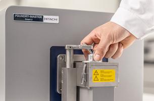
Hitachi High-Tech have developed XRF analyzers specifically suited to verifying IC substrates, under bump metallurgy, lead frame plating and PCB plating. The FT160 analyzer includes the latest X-ray technology to deliver high-precision measurements of nanometer-scale plating. A beam diameter of less than 30 µm allows for highly accurate plating thickness measurements and composition analysis, essential for solder bumps, metal deposits and plating throughout semiconductor fabrication.
Find out more Get in touch