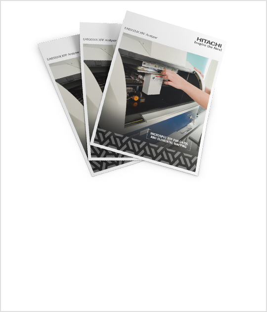
Our range of high-precision XRF analyzers for semiconductor wafers are ideal for coating thickness analysis on flip chip packaging and IC substrates. Precisely locate and analyze coating thicknesses for metallization, ball grid arrays (BGA), solder bump and under bump metallurgy. Easily and accurately analyze gold (Au), silver (Ag), tin (Sn), titanium (Ti) and chrome (Cr) from plating, CVD and PVD operations. Depending on your choice of optics technology, you can reliably measure down to the nanometer level for wafer features smaller than 50 µm (micron).
Request Pricing or Demo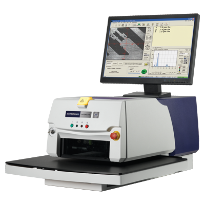
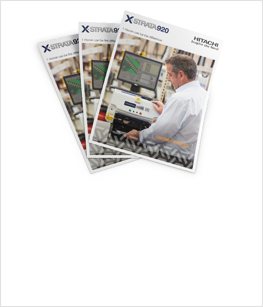
X-Strata920: Flexible fit for different sized samples
Designed to analyze wafers in a range of sizes, the X-Strata920 is ideal for many applications, coating thickness analysis of semiconductor wafers.
Download brochure X-Strata920 SDD: Flexibility with high resolution detector
The X-Strata920 SDD offers the same flexibility as the X-Strata920, but with a silicon drift detector (SDD) for analyzing complex and thinner coatings.
Download brochure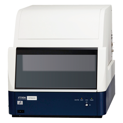
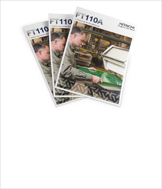
FT110A: Powerful XRF for large samples
Designed to accommodate larger samples, this advanced XRF analyzer is easy to use and delivers fast and accurate results, with features built for high productivity.
Download brochure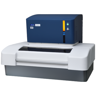
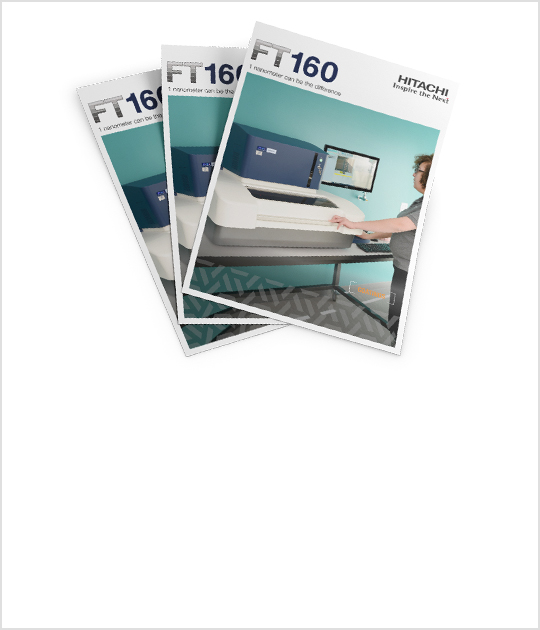
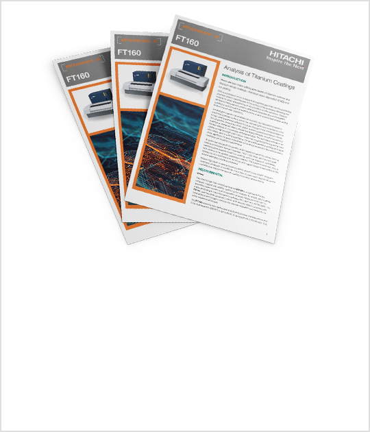
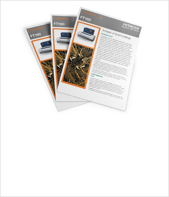
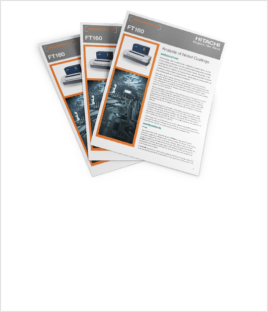
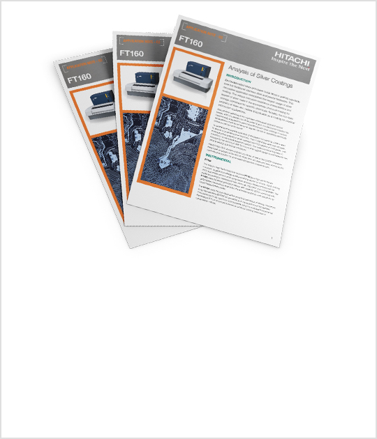
FT160: Microspot analysis for miniaturized electronics
Designed for microspot and ultra-thin coatings analysis, the FT160’s polycapillary optics and detector technology are optimized for features less than 50 µm.
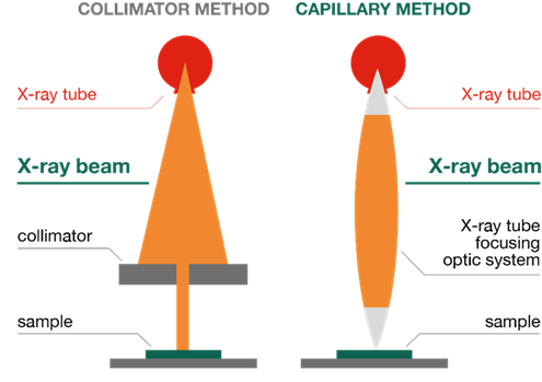
Download brochureChoose from two optics configurations: mechanical collimators or polycapillary optics, depending on the size of your wafer features and thickness of the coatings you need to analyze.
Collimators:
Ideal for features down to 100 µm, our analyzers with collimators offer multiple size options for optimized precision.
Capillary optics:
For features less than 100 µm and coatings in the nanometer-range, capillary optics are best. For our polycapillary optics XRF instruments, several capillary tubes are clustered together in a tapered configuration. This advanced technology can achieve the smallest spot sizes and direct more X-rays at the board, giving better precision on smaller areas.
| X-Strata920 | X-Strata920 | FT110A | FT160 | |
| Au plating | ★★☆ | ★★★ | ★★☆ | ★★★ |
| Ag plating | ★★☆ | ★★★ | ★★☆ | ★★★ |
| Sn plating | ★★☆ | ★★★ | ★★☆ | ★★★ |
| Ti plating | ★★☆ | ★★★ | ★★☆ | ★★★ |
| Cr plating | ★★☆ | ★★★ | ★★☆ | ★★★ |
| CVD, PVD coatings | ★☆☆ | ★★☆ | ★☆☆ | ★★★ |
| BGA composition analysis | ★★☆ | ★★★ | ★★☆ | ★★★ |
| Thin film analysis at nm-scale | N/A | ★★☆ | N/A | ★★★ |
| Measure features < 50 µm | N/A | N/A | N/A | ★★★ |
| Automated focus | N/A | N/A | ★★★ | ★★★ |
| Wide-view camera | N/A | N/A | ★★★ | N/A |
| Pattern recognition | N/A | N/A | ★★★ | ★★★ |
Our global experts are on hand to help your business find the XRF analyzer for your needs.