Our range of high-performance benchtop XRF instruments is designed for coating thickness analysis of metal surface finishes (final finishes). Measure coating thicknesses of gold (ENIG, ENEPIG), immersion silver, immersion tin and hot air solder leveling HASL (including lead-free) finishes on wide range of substrates, including PCB/PWB, rigid board, flex board (FPC) and rigid-flex board. Ultra-high precision and accuracy, together with an intuitive interface, makes it easy to get reliable results fast, even down to the nanometer level.
Request Pricing or Demo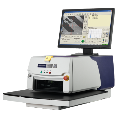
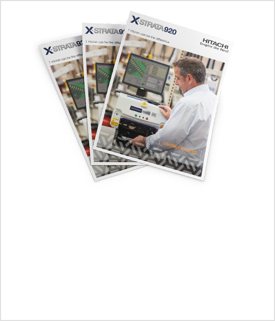
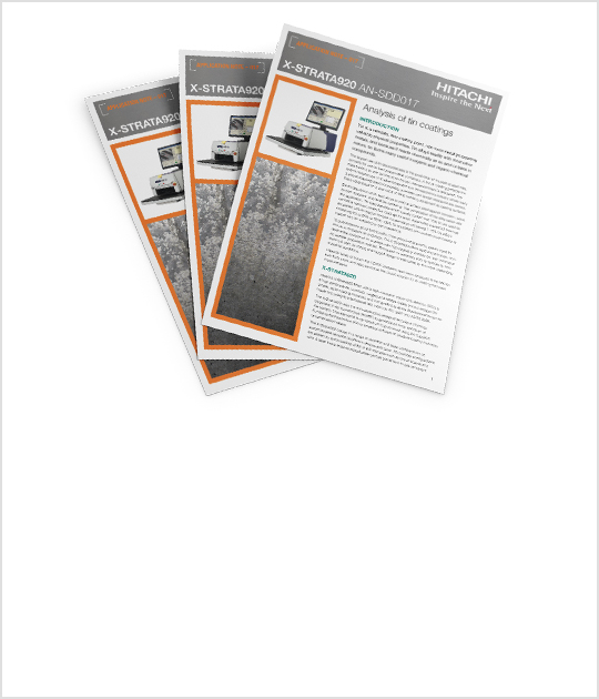
X-Strata920: Flexible fit for samples of any shape
Designed to analyze samples of a wide variety of shapes and sizes, the X-Strata920 is ideal for many applications, including PCB surface finishes.
Download the brochure X-Strata920 SDD: Flexibility with high resolution detector
The X-Strata920 SDD offers the same flexibility as the X-Strata920, but with a silicon drift detector (SDD) for analyzing complex and thinner coatings.
Download the brochure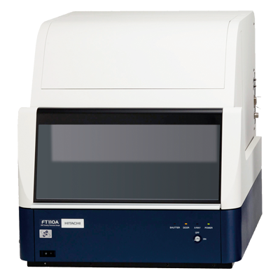
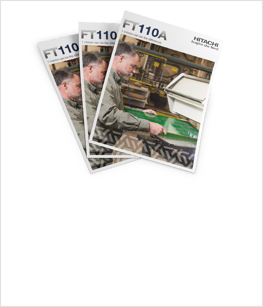
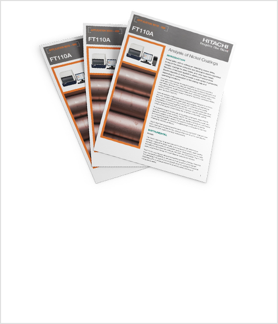
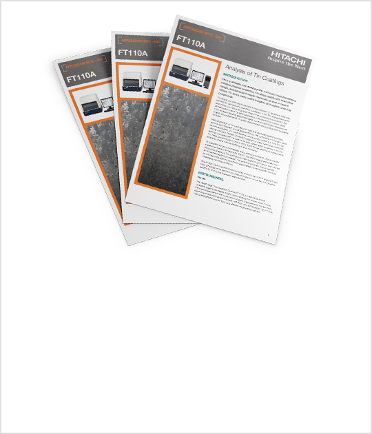
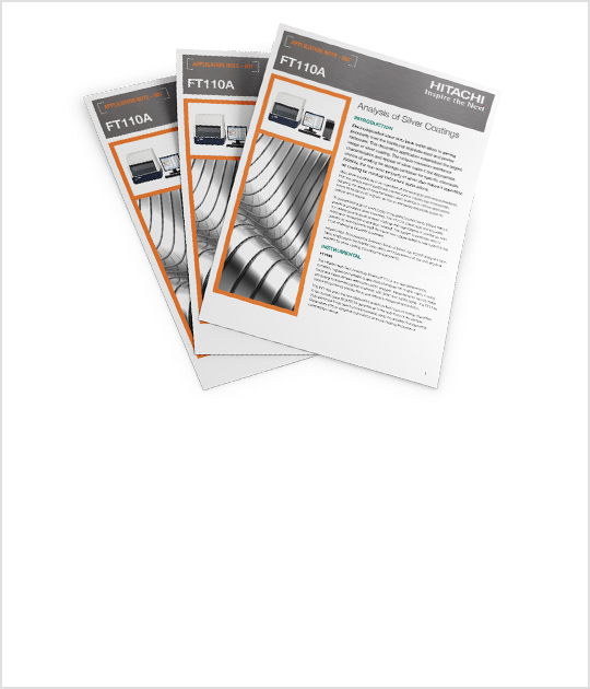
FT110A: Powerful XRF for larger boards
Designed to accommodate large boards, this advanced XRF analyzer is easy to use and delivers fast and accurate results with features built for high productivity.
Download the brochure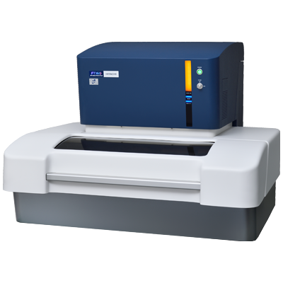
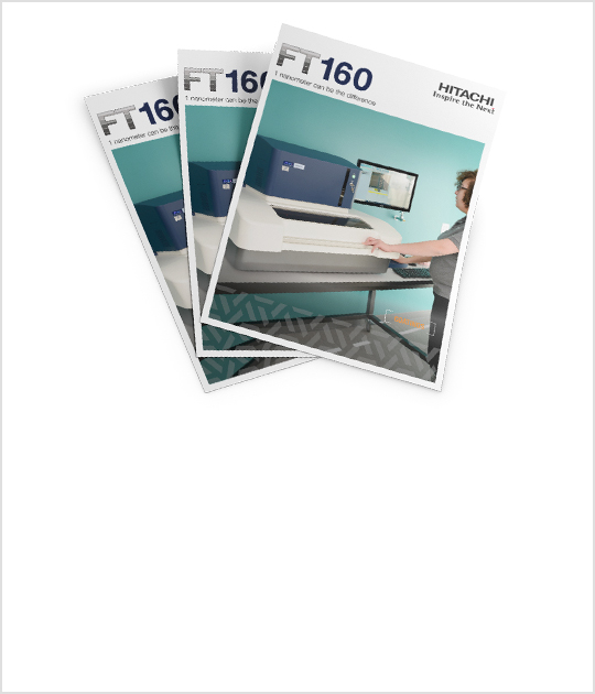
FT160: Microspot analysis for miniaturized electronics
Designed for microspot and ultra-thin coatings analysis, the FT160’s polycapillary optics and detector technology are optimized for features less than 50 µm.
Download the brochure- Verify plating thickness is within the lower and upper specification limits for gold (Au) and electroless nickel (NiP) with XRF.
- Meet the Type 1 Gage performance required to satisfy the requirements of IPC-4552B
- Ensure your silver (Ag) coatings fall within the lower and upper thickness specifications.
- Understand how your detector selection affects setup and performance.
- Meet the minimum total tin (Sn) thickness to meet the immersion tin IPC specification.
- This standard calls for differentiation between total tin thickness and useable tin thickness.
- Measure the lower limits for gold (Au), lower and upper limits for palladium (Pd), and lower and upper limits for electroless nickel (NiP).
- Meet the required XRF Type 1 Gage performance criteria for this IPC specification.
| X-Strata920 | X-Strata920 | FT110A | FT160 | |
| ENIG | ★★☆ | ★★★ | ★★☆ | ★★★ |
| ENIG (IPC-4552B) | ★☆☆ | ★★☆ | ★☆☆ | ★★★ |
| ENEPIG (IPC-4556) | ★☆☆ | ★★☆ | ★☆☆ | ★★★ |
| Immersion Sn | ★★☆ | ★★★ | ★★☆ | ★★★ |
| Immersion Ag | ★★☆ | ★★★ | ★★☆ | ★★★ |
| HASL | ★★☆ | ★★★ | ★★☆ | ★★★ |
| Electroless nickel thickness | ★★★ | ★★★ | ★★★ | ★★★ |
| Electroless nickel thickness and composition | N/A | ★★☆ | N/A | ★★★ |
| Thin film analysis at sub-micron scale | ★☆☆ | ★★☆ | ★☆☆ | ★★★ |
| Measure features < 100 µm | ★☆☆ | ★☆☆ | ★☆☆ | ★★★ |
| Automated focus | N/A | N/A | ★★★ | ★★★ |
| Wide-view camera | N/A | N/A | ★★★ | N/A |
| Pattern recognition | N/A | N/A | ★★★ | ★★★ |
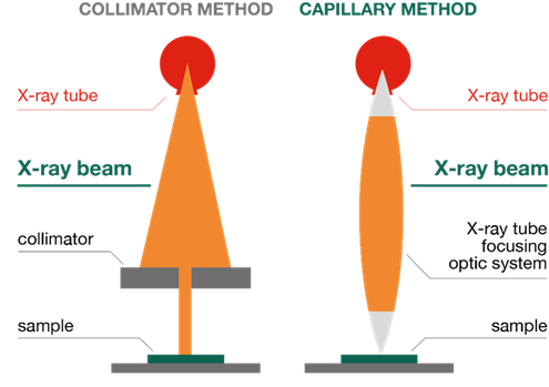
Choose from two optics configurations: mechanical collimators or polycapillary optics, depending on the size of your board features and thickness of the coatings you need to analyze.
Ideal for features down to 100 µm, our analyzers with collimators offer multiple size options for optimized precision and rapid analysis.
For features less than 100 µm and coatings in the nanometer-range, capillary optics are the best choice. For our polycapillary optics XRF instruments, many capillary tubes are clustered together in a tapered configuration. This advanced technology can achieve the smallest spot sizes and direct more X-rays at the board, giving better precision on smaller areas.
Our global experts are on hand to help your business find the XRF analyzer for your needs.
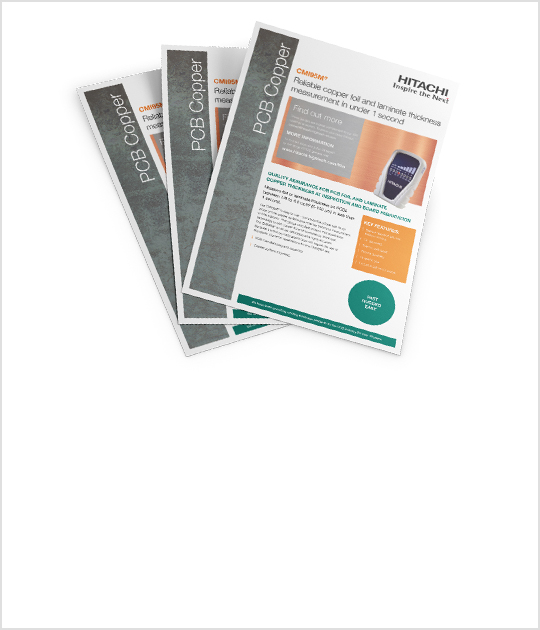
CMI95M: Rapid and reliable copper foil and laminate thickness measurement
Measure foil or laminate thickness on PCBs between 1/8 to 4.0 oz/ft2 (5-140 μm) in less than 1 second.
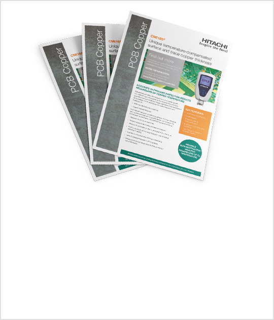
CMI165: Reliable and non-destructive analysis regardless of copper (Cu) temperature
Unique temperature-compensated surface and trace copper (Cu) thickness measurement.
CMI511: Rapid measurement of thru-hole copper (Cu) thickness at any temperature
Temperature compensation allows for fast measurement of plated thru-hole copper (Cu) thickness prior to, and after, etching.
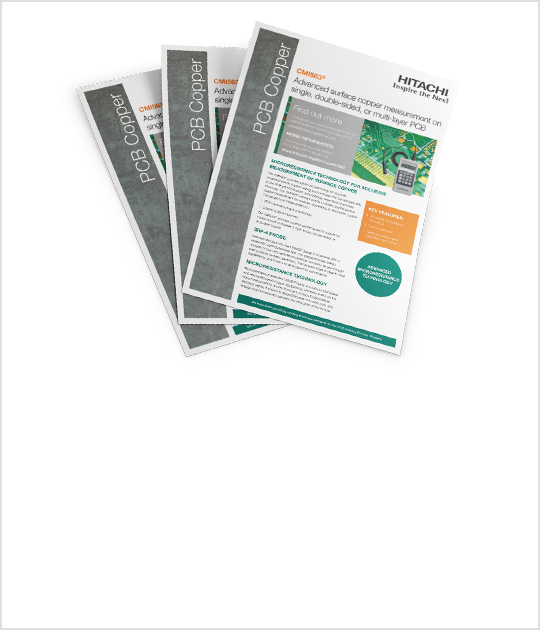
CMI563: Microresistance technology for accurate measurement of copper (Cu)
Advanced surface copper (Cu) measurement on single, double-sided or multi-layer PCB
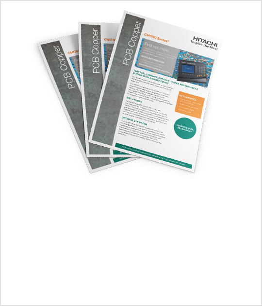
CMI760: Dual technology for multiple PCB copper (Cu) applications
Dual eddy current and microresistance technology enables you to test foil, laminate, surface, traces and thru-hole copper (Cu) with a single device.
| Model | CMI95M | CMI165 | CMI511 | CMI563 | CMI760 |
| Technique | Microresistance | Microresistance | Eddy | Microresistance | Microresistance |
| Copper Foil | ✔ | ✔ | ✔ | ✔ | |
| Copper Laminate | ✔ | ✔ | ✔ | ✔ | |
| Copper - Surface | ✔ | ✔ | ✔ | ||
| Copper - Fine Line | ✔ | ✔ | ✔ | ||
| Copper Thru-hole | ✔ | Optional | |||
| Temperature Compensation | ✔ | ✔ | ETP Probe | ||
| Replacement Probe Tip | N/A | ✔ | ✔ | SRP-4 Probe | |
| Unit Selection | oz or µm | mil or µm | mil or µm | mil or µm | mil or µm |
| Copper Thickness Range - µm | 8 indicator lights: 5-140 | Electroless: | 2-102 | Electroless: | Surface: |
| Copper Thickness Range - mil | Electroless: 0.01-0.5 Electroplated: 0.1-10 | 0.08-4 | Electroless: 0.01-0.5 Electroplated: 0.01-6 | Surface: 0.01-10 Thru-hole: 0.08-4 |