The performance and cost of commercial spark optical emission spectrometer (OES) instruments depends on many things, but a huge part of this is the detector technology within the instrument.
Complementary metal oxide semiconductor (CMOS) detectors have been developed for the latest generation of OES analyzers, taking over from photomultiplier tube (PMT), a vacuum technology still manufactured for industrial use, and semiconductor-based charge coupled device (CCD).
Here’s why manufacturers, like ourselves, are choosing CMOS detectors to ensure flexibility so we can ensure our customers are always equipped with the latest software.
Optical emission spectroscopy in simple terms creates a localized plasma at the analysis site and the optical spectrum of this plasma tells us which elements are present in the sample. All OES detectors must be capable of detecting these optical signals and converting them into something that can be measured (electrical signals). All detectors rely on the photoelectric effect to convert the incident light into electrical current.
However, the type of material used for the detection and the subsequent amplification method of the photo-generated electrons into something we can measure is different for the between detector technologies. Until recently, the detector technology of choice for OES was between either PMT or CCD.
Photomultiplier tubes are essentially vacuum tubes that accelerate and amplify the generated electrons, whereas CCDs are an array of many light-sensitive pixels that are fully integrated into a complete semiconductor device that is directly connected to the rest of the detection electronics.
PMTs can be seen as highly specialized detectors that detect the presence of a few, specific elements to very low detection limits, whereas CCDs can cover a wider range of elements. The trade-off is that the level of sensitivity is lower, so they are not good for areas (like melt analysis) where you must control tramp and trace elements to very low limits.
CMOS is a semiconductor topography technology that’s been in widespread use in integrated circuits. Its main advantage over the original bipolar transistor technology is high speed and almost zero static power dissipation - meaning that more devices can be crammed into a small space without everything overheating. This is why CMOS-based devices dominate microprocessors, RAM, and ASICs (to name a few) today.
When it comes to using CMOS technology in light detection, the devices work in a very similar way to CCDs. There’s an array of photosensitive pixels that convert incident light over many wavelengths into electrical signals.
CMOS isn’t new, but the technology has recently developed to make it even more efficient and less noisy for optical applications. And, as CMOS production is so widespread, it’s relatively cheap compared with specialist CCD manufacturing, which is why camera manufacturers are starting to choose CMOS over CCD for the image capture part of their DSLRs.
The CMOS chip is also fast in multiplexed readout electronics. This enables it to be used in areas where speed matters, like analytical tasks.
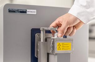
Our OES instruments use CCDs (charge coupled devices) except for our latest OE Series, which uses CMOS detectors. Both detector types are semiconductor-based and can be tailored to cover the whole spectrum within optical systems.
The OE Series combines the range and sensitivity of CMOS-based detectors with a brand-new optical design to deliver a level of performance usually only possible with much higher cost instruments. With low operating costs and a relatively small footprint, the OE Series can detect the entire spectrum of elements within metals, including gasses (the OE 750).
For OE720 the wavelength covered is 174-690nm whilst for the OE750, the CMOS detector covers 119nm up to 766nm, which means it can analyze all relevant elements within metals, from hydrogen upwards. This is because CMOS detectors have a very good resolution, dynamic range, and are very linear. They’re optimized for measuring UV light and can also be used for TRS (time resolved spectroscopy).
Find out more about the OE Series or get in touch with our experts for a discussion about how the OE Series could help your business.
Find out more Get in touchYou might also be interested in: