XRF analysis is the technique of choice for verifying the thickness and composition of coatings on electronic devices. Accurate, precise, fast and non-destructive, XRF ensures that multilayer coatings will perform well over the expected shelf life of the component. If you’re adhering to IPC guidelines, then XRF is the technique of choice for many of their specifications.
However, while the analysis time for XRF is a matter of seconds, the setup time can be far longer. And this is especially the case in the field of electronics, when you have to locate minute features on a large substrate or PCB. Many of these features need a microscope to see them properly, and this means lots of frustrating zooming in and out and moving the sample around, then checking and re-checking before the analysis button is pressed. The good news is that many XRF instruments have features that are designed to make sample setup much faster and we’re going to take a look at three of them here.
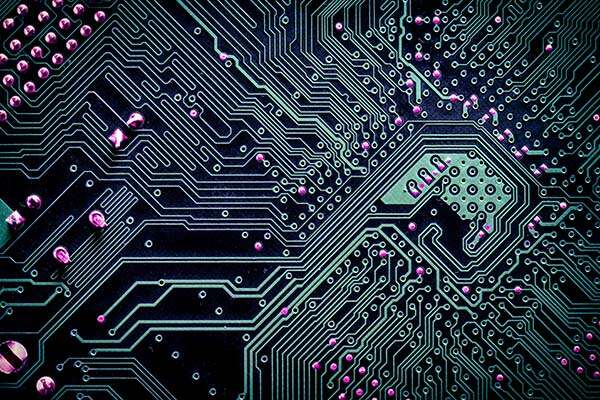
Even when you are fully zoomed out, you may still find it difficult to navigate around your sample, simply because you can’t see all of it in the image window. Using a wide-view camera allows you to see the whole PCB at once. Then, you can go to the right area of interest before zooming in and viewing the part on the micro level. This is especially useful when you are measuring several different points across a large substrate.
In our testing, we’ve found that you can achieve a 20% time saving when using a wide-view camera against a standard, narrow view one.
Some XRF instruments have pattern recognition software installed and this can help enormously when finding the right analysis location on large substrates. This is useful when you are measuring large parts that are all the same, for example a batch of PCBs.
Essentially, image processing software recognizes patterns on your substrate and the automated stage positions your sample into the right position. There is some setting up involved, you’ll have to teach the software which pattern look for, but you will save a lot of time if you have a lot of identical parts to analyze. Not only does this save you time, but it also reduces the likelihood of error as the measurements are always taken in the right location.
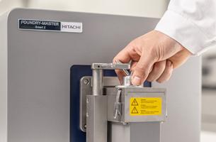
Once the substrate is in the correct location for analysis, the next setup step is to ensure it is focused correctly. In XRF, the distance between the X-ray source, the sample and the detector must be a known distance for the results to be accurate. Different instruments deal with this differently. On a basic level, the operator can manually focus the instrument, which involves manually moving the head of the instrument until the part is in focus (usually by aligning a laser spot on the substrate). However, some XRF instruments automatically move the instrument head to the right focal distance. This saves a lot of time for the operator and, as maintaining the right distance is essential for reliable results, reduces the likelihood of error in the measurement.
We put manual vs automated to the test and found that you can save up to a third of your time when switching to automated focusing over the manual technique.
You can get more detail on these time-saving methods in our free guide: Understanding your XRF: A Guide for Electronics Plating.
Written specifically for those measuring electronics coatings with XRF, this comprehensive guide covers everything XRF, from the fundamentals of the technique to how to get more reliable results.
You can learn:
You can download your free copy here.
Get in touch